تم الحل ✓
categoryالهندسة الكهربائية
schoolبكالوريوس
event_available2026-07-14
السؤال
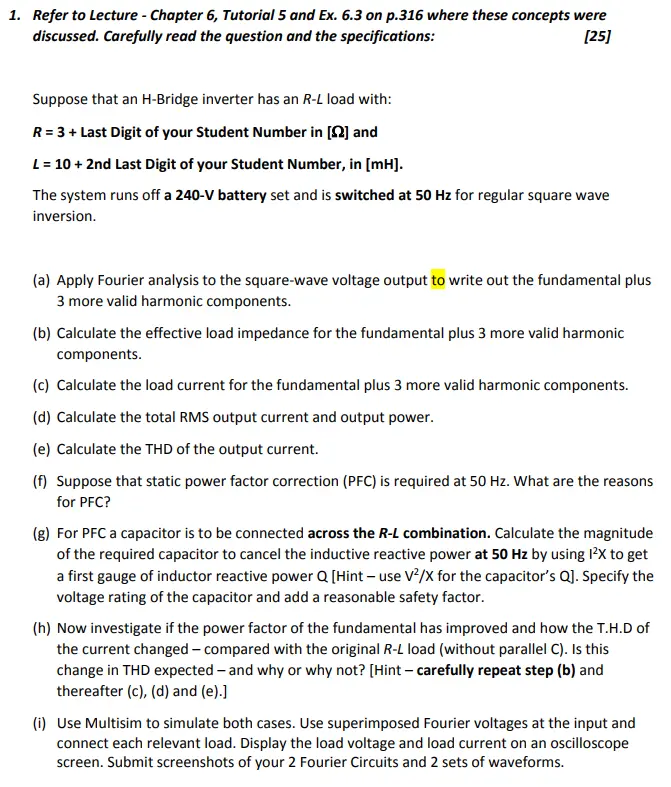
Transcribed Image Text:
1. Refer to Lecture - Chapter 6, Tutorial 5 and Ex. 6.3 on p.316 where these concepts were
discussed. Carefully read the question and the specifications:
[25]
Suppose that an H-Bridge inverter has an R-L load with:
R = 3 + Last Digit of your Student Number in [2] and
L = 10 + 2nd Last Digit of your Student Number, in [MH].
The system runs off a 240-V battery set and is switched at 50 Hz for regular square wave
inversion.
(a) Apply Fourier analysis to the square-wave voltage output to write out the fundamental plus
3 more valid harmonic components.
(b) Calculate the effective load impedance for the fundamental plus 3 more valid harmonic
components.
(c) Calculate the load current for the fundamental plus 3 more valid harmonic components.
(d) Calculate the total RMS output current and output power.
(e) Calculate the THD of the output current.
(f) Suppose that static power factor correction (PFC) is required at 50 Hz. What are the reasons
for PFC?
(g) For PFC a capacitor is to be connected across the R-L combination. Calculate the magnitude
of the required capacitor to cancel the inductive reactive power at 50 Hz by using I²x to get
a first gauge of inductor reactive power Q [Hint - use V²/X for the capacitor's Q]. Specify the
voltage rating of the capacitor and add a reasonable safety factor.
(h) Now investigate if the power factor of the fundamental has improved and how the T.H.D of
the current changed - compared with the original R-L load (without parallel C). Is this
change in THD expected - and why or why not? [Hint - carefully repeat step (b) and
thereafter (c), (d) and (e).]
(i) Use Multisim to simulate both cases. Use superimposed Fourier voltages at the input and
connect each relevant load. Display the load voltage and load current on an oscilloscope
screen. Submit screenshots of your 2 Fourier Circuits and 2 sets of waveforms.
Example 6.3 Finding the Output Voltage and Current of a Single-Phase
Full-Bridge Inverter with an RLC Load
The bridge inverter in Figure 6.3a has an RLC load with R = 100, L = 31.5mH, and C = 112 μF.
The inverter frequency is fo = 60 Hz and de input voltage is V, = 220 V. (a) Express the instan-
taneous load current in Fourier series. Calculate (b) the rms load current at the fundamental
frequency I,1, (c) the THD of the load current, (d) the power absorbed by the load Po and the
fundamental power P01, (e) the average current of de supply I,, and (f) the rms and peak current
of each transistor. (g) Draw the waveform of fundamental load current and show the conduction
intervals of transistors and diodes. Calculate the conduction time of (h) the transistors, (i) the
diodes, and (j) the effective load angle 0.
Solution
V₁ = 220 V, fo=60 Hz, R = 102, L = 31.5mH, C = 112 μF, and w = 2 X 60377 rad/s.
The inductive reactance for the nth harmonic voltage is
XL = jwL = j2nm × 60 × 31.5 x 103 = j11.87n
The capacitive reactance for the nth harmonic voltage is
j106
-j23.68
X
пос
2nπ X 60 X 112
n
The impedance for the nth harmonic voltage is
Zn
R²+noL
L-11)² = [10² + (11.87n - 23.68/n) 312
and the load impedance angle for the nth harmonic voltage is
On
= tan
11.87n - 23.68/n
10
=tan
tan ¹(1.187n –
2.368
n
a. From Eq. (6.16), the instantaneous output voltage can be expressed as
v(t) =280.1 sin (377) + 93.4 sin (3 x 3771) + 56.02 sin (5 × 3771)
+ 40.02 sin (7 x 377t) + 31.12 sin (9 x 3771) + ...
Dividing the output voltage by the load impedance and considering the appropri-
ate delay due to the load impedance angles, we can obtain the instantaneous load
current as
i(t) = 18.1 sin (377 +49.72°) + 3.17 sin (3 × 3771 - 70.17°)
+ sin (5 x 3771-79.63°) + 0.5 sin (7 × 3771 - 82.85°)
+ 0.3 sin (9 x 3771 - 84.52°) +
b. The peak fundamental load current is Im₁ = 18.1A. The rms load current at funda-
mental frequency is I1 = 18.1/V2 = 12.8 A.
c. Considering up to the ninth harmonic, the peak load current,
Im = (18.1² + 3.17² + 1.0² + 0.5² + 0.32) 1/2 = 18.41 A
The rms harmonic load current is
In
(P)
√2
1/2
m1
18.41² – 18.12
νε
2.3789A
Using Eq. (6.6), the THD of the load current is
THD
(P-1) 1/2
Im1
= [(18.41)² - 1]'² =
11/2
= 18.59%
d. The rms load current is I = IV2 = 18.41/√2 = 13.02 A, and the load power is
Po = 13.022 x 10 = 1695 W. Using Eq. (6.13), the fundamental output power is
Pol R = 12.82 x 10 = 1638.4W
=
=
e. The average supply current I, PV,
1695/220 7.7 A.
f. The peak transistor current I, I = 18.41 A. The maximum permissible rms
current of each transistor is Io(max) = 1/√√2 = 1/2 = 18.41/2 = 9.2A.
g. The waveform for fundamental load current i₁(t) is shown in Figure 6.4.
h. From Figure 6.4, the conduction time of each transistor is found approximately from
wto = 180 49.72 = 130.28° or to 130.28 X π/(180 × 377) = 6031 μs.
i. The conduction time of each diode is approximately
ta (180 130.28) X
πT
= 2302 μs
180 x 377
j. The effective load angle can be found from
Volo cos 0 = Po or 220 x 13.02 x cos 0 = 1695
which gives 53.73°
25
BEC
21.14
20
i(t)
i(t)
15
10
Fundamental
current, io1
16.667 ms
ta = 2.639 ms
5
8.333 ms
0
-5
1.944 ms
1.8638 ms
-10-
5.694 ms
-15
-20
Q₁ on
D₁
on
-25
Q₂ on
D2
on
FIGURE 6.4
Waveforms for Example 6.3.
Notes:
1. To calculate the exact values of the peak current, the conduction time of transis-
tors and diodes, the instantaneous load current i,(t) should be plotted as shown
in Figure 6.4. The conduction time of a transistor must satisfy the condition
io(t = to) = 0, and a plot of i,(t) by a computer program gives Ip = 21.14A,
to = 5694 μs, and t₁ = 2639 μs.
2. This example can be repeated to evaluate the performance of an inverter with R, RL,
or RLC load with an appropriate change in load impedance Z and load angle 0,.
Gating sequence. The gating sequence for the switching devices is as follows:
1. Generate two square-wave gating signals 1 and 2 at an output frequency fo
and a 50% duty cycle. The gating signals Vg3 and vg4 should be the logic invert of
Vg1 and vg2, respectively.
2. Signals Vg1 and Vg3 drive Q₁ and Q3, respectively, through gate isolation circuits.
Signals Vg2 and vg4 can drive Q2 and Q4, respectively, without any isolation circuits.
check_circle الجواب — حل مفصل خطوة بخطوة
hourglass_top
🔒
الحل الكامل متاح للمشتركين
اشترك في أرشيف الأسئلة لعرض هذا الحل وآلاف الحلول المفصلة خطوة بخطوة من معلمين معتمدين.