تم الحل ✓
categoryهندسة كهربائية
schoolبكالوريوس
event_available2026-07-14
السؤال
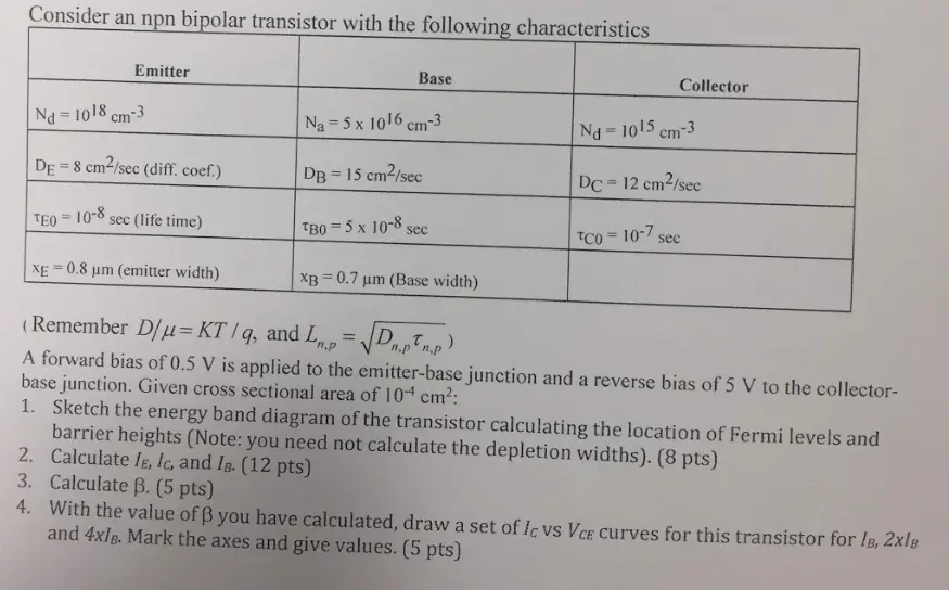
Transcribed Image Text:
Consider an npn bipolar transistor with the following characteristics
Emitter
Base
Collector
Nd=1018 cm-3
Na = 5 x 1016 cm-3
Nd=1015 cm-3
DE
= 8 cm²/sec (diff. coef.)
TEO 10-8.
=
DB = 15 cm²/sec
DC = 12 cm²/sec
sec (life time)
TB0 = 5 x 10⁻⁸ sec
TCO = 10-7 sec
=
XE 0.8 μm (emitter width)
XB 0.7 μm (Base width)
(Remember D/μ=KT/q, and Ln.p=√√D.pn.p)
A forward bias of 0.5 V is applied to the emitter-base junction and a reverse bias of 5 V to the collector-
base junction. Given cross sectional area of 104 cm²:
1. Sketch the energy band diagram of the transistor calculating the location of Fermi levels and
barrier heights (Note: you need not calculate the depletion widths). (8 pts)
2. Calculate IE, Ic, and IB. (12 pts)
3. Calculate ẞ. (5 pts)
4. With the value of ẞ you have calculated, draw a set of Ic vs VCE curves for this transistor for IB, 2xlB
and 4xlB. Mark the axes and give values. (5 pts)
check_circle الجواب — حل مفصل خطوة بخطوة
hourglass_top
🔒
الحل الكامل متاح للمشتركين
اشترك في أرشيف الأسئلة لعرض هذا الحل وآلاف الحلول المفصلة خطوة بخطوة من معلمين معتمدين.