تم الحل ✓
categoryهندسة كهربائية
schoolبكالوريوس
event_available2026-07-14
السؤال
Transcribed Image Text:
The Transfer Characteristic
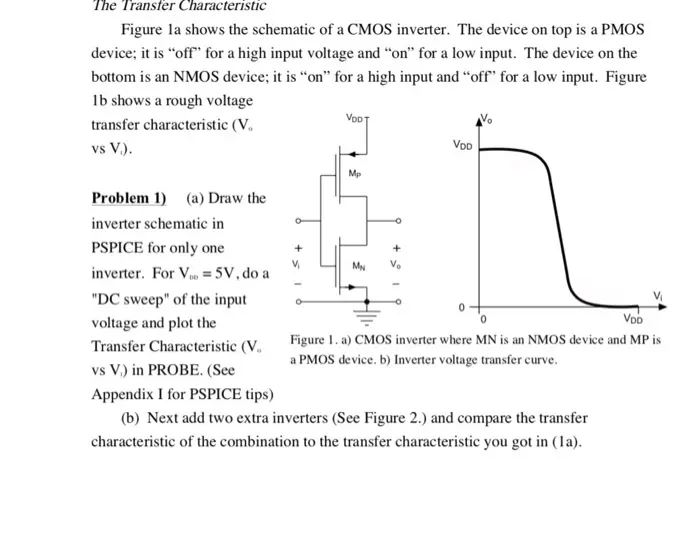
Figure la shows the schematic of a CMOS inverter. The device on top is a PMOS
device; it is "off" for a high input voltage and "on" for a low input. The device on the
bottom is an NMOS device; it is "on" for a high input and "off" for a low input. Figure
lb shows a rough voltage
transfer characteristic (V.
vs V.).
Problem 1) (a) Draw the
inverter schematic in
VOOT
Mp
VDD
PSPICE for only one
inverter. For V = 5V, do a
"DC sweep" of the input
voltage and plot the
Transfer Characteristic (V.
vs V.) in PROBE. (See
Appendix I for PSPICE tips)
MN
VDD
Figure 1. a) CMOS inverter where MN is an NMOS device and MP is
a PMOS device. b) Inverter voltage transfer curve.
(b) Next add two extra inverters (See Figure 2.) and compare the transfer
characteristic of the combination to the transfer characteristic you got in (1a).
check_circle الجواب — حل مفصل خطوة بخطوة
hourglass_top
🔒
الحل الكامل متاح للمشتركين
اشترك في أرشيف الأسئلة لعرض هذا الحل وآلاف الحلول المفصلة خطوة بخطوة من معلمين معتمدين.