تم الحل ✓
categoryهندسة كهربائية
schoolبكالوريوس
event_available2026-07-13
السؤال
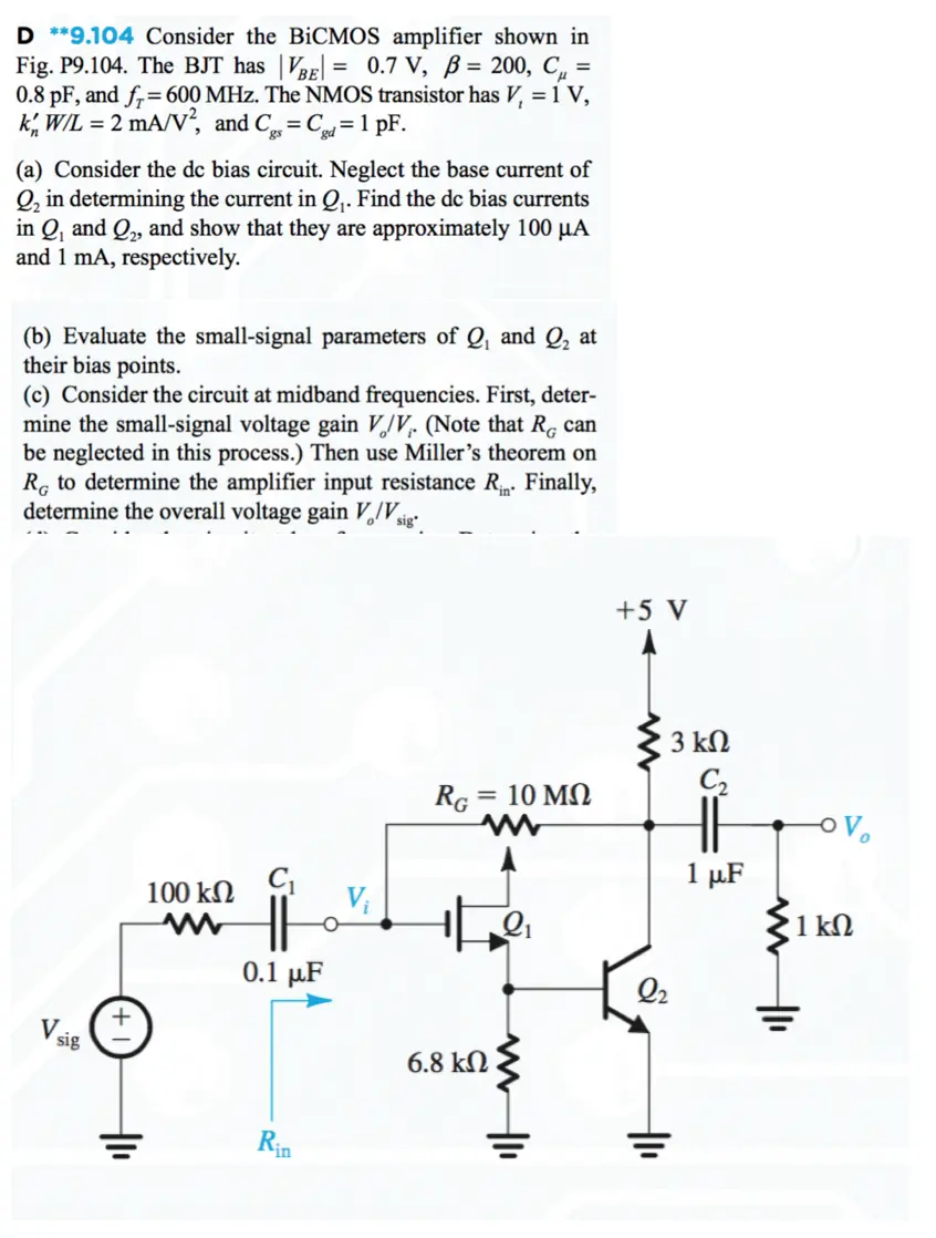
Transcribed Image Text:
=
D **9.104 Consider the BiCMOS amplifier shown in
Fig. P9.104. The BJT has | VBE| = 0.7 V, B = 200, Cμ
0.8 pF, and fr=600 MHz. The NMOS transistor has V, = 1 V,
kW/L = 2 mA/V2, and C = C = 1 pF.
(a) Consider the dc bias circuit. Neglect the base current of
Q2 in determining the current in Q₁. Find the dc bias currents
in Q, and Q2, and show that they are approximately 100 μА
and 1 mA, respectively.
(b) Evaluate the small-signal parameters of Q, and Q₂ at
their bias points.
(c) Consider the circuit at midband frequencies. First, deter-
mine the small-signal voltage gain V/V. (Note that Rc can
be neglected in this process.) Then use Miller's theorem on
RG to determine the amplifier input resistance R. Finally,
determine the overall voltage gain V/V sig
V sig
+5 V
w
3 ΚΩ
C₁₂
RG
= 10 ΜΩ
w
-OV
100 ΚΩ
C₁
1 µF
V₁
O
Q1
1 ΚΩ
0.1 µF
Q2
Rin
6.8 ΚΩ
check_circle الجواب — حل مفصل خطوة بخطوة
hourglass_top
🔒
الحل الكامل متاح للمشتركين
اشترك في أرشيف الأسئلة لعرض هذا الحل وآلاف الحلول المفصلة خطوة بخطوة من معلمين معتمدين.