تم الحل ✓
categoryهندسة كهربائية
schoolبكالوريوس
event_available2026-07-14
السؤال
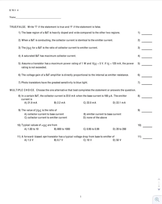
Transcribed Image Text:
1)
2)
=23
3)
4)
5)
HW# 4
Name
TRUE/FALSE. Write "T" if the statement is true and 'F' if the statement is false.
1) The base region of a BJT is heavily doped and wide compared to the other two regions.
2) When a BJT is conducting, the collector current is identical to the emitter current.
3) The BDC for a BJT is the ratio of collector current to emitter current.
4) A saturated BJT has maximum collector current.
5) Assume a transistor has a maximum power rating of 1 W and VCE -5 V. If Ic = 120 mA, the power
rating is not exceeded.
6) The voltage gain of a BJT amplifier is directly proportional to the internal ac emitter resistance.
7) Photo transistors have the greatest sensitivity to blue light.
6)
7)
MULTIPLE CHOICE. Choose the one alternative that best completes the statement or answers the question.
8) In a certain BJT, the collector current is 22.0 mA when the base current is 100 pA. The emitter
current is
A) 21.9 mA
B) 2.2 mA
C) 22.0 mA
8)
D) 22.1 mA
9) The value of BDC is the ratio of
A) collector current to base current
C) collector current to emitter current
10) Typical values of aDC are from
A) 1.00 to 10
B) 800 to 1000
B) emitter current to base current
D) none of the above
C) 0.95 to 0.99
01
10)
D) 20 to 200
11)
D) 50 V
11) A forward-biased npn transistor has a typical voltage drop from base to emitter of
A) 1.5 V
B) 0.7 V
C) 10 V
4-10▸
R₁
R180
BB
VR+
ww
33 ΚΩ
6 V
Figure 1
Voc
15 V
12) Refer to Figure 1. Assume BDC 200. The expected value of IB is
A) 161 A
B) 182 A
C) 200 μA
13) Refer to Figure 1. Assume BDC - 200. The value of VCE is approximately
A) 5.8 V
B) 9.2 V
14) Refer to Figure 1. If VCC is increased to 18 V. IB will
C) 7.5 V
A) increase
B) decrease
12)
D) 80 A
13)
D) 12.4 V
14)
C) not change
VCE
0.7 V
Figure 2 A characteristic curve
15) For the characteristic curve in Figure 2, the region between A and B is called the
A) breakdown region
C) cutoff region
B) active region
D) saturation region
16) For the characteristic curve in Figure 2, the equation IC BDC/B is true
A) only beyond C on the curve
C) only between B and C on the curve
17) ICEO is
A) collector current when the transistor is cutoff
B) base current when the transistor is saturated
C) collector current when the transistor is on
D) collector current when the transistor is saturated
18) If a BJT is saturated.
15)
16)
B) at no place on the curve
D) only between A and B on the curve
17)
A) both base current and collector current are at a maximum
B) VCC appears between the collector and emitter
C) base current is at maximum
D) collector current is at maximum
19) If a BJT is saturated.
A) VCE is approximately 1/2 VCC
C) VCE is near zero
18)
19)
B) VCE is approximately equal to VCC
D) none of the above
3
V₁
BB+
2.5 V
Re≥500
RB
Voc
ww
18 ΚΩ
Boc-200
Figure 3 The transistor has the following ratings: PD (max) = 650 mW. VCE (max) = 40 V. and IC(max) = 200 mA.
20) Refer to Figure 3. The maximum value that VCC can be adjusted to without exceeding the
VCE(max) rating is (ignore other max ratings).
A) 60 V
B)
40 V
C) 45 V
21) Refer to Figure 3. If VCC is set to 48 V. PD(max) is exceeded by
A) 110 mW
B) 80 mW
20
D) 50 V
21)
C) 310 mW
D) 55 mW
22)
C) in the linear range
23)
C) Av
D) PD(max)
22) Refer to Fig 3. Assume VCC is lowered to 15 V. The transistor is
A) cutoff
B) saturated
23) The symbol hFE means the same as
B) BDC
A) DC
24) HFE varies with
A) temperature
B) collector current
C) both A and B
D) none of the above
25) A 10 mV ac signal is applied to the base of a properly biased transistor with RC = 1.2k and r =
36. The output ac voltage is
A) 152 mV
B) 33 mV
C) 333 mV
D) 105 mV
24)
220
25)
VBB 4.0 V
RB
ww
Κ Ε 1.5 ΚΩ
Vcc=15 V
Poc=100
Figure 4
26) Refer to Figure 4. Assume RB-22 kg. The collector current will be approximately
A) 10 mA
B) 5 mA
C) 20 mA
27) Refer to Figure 4. The largest base resistor that will still saturate the transistor is approximately
Α) 33 ΚΩ
Β) 330 ΚΩ
28) Refer to Figure 4. If RB-100 k2, Vc is approximately
A) 12.5 V
B) 10 V
C) 40 k
C) 7.5 V
26)
D) 27 mA
27)
D) 400 k
28)
D) 5 V
29)
29) Refer to Figure 4. If you wanted to change the transistor to a pnp type, you need to
A) increase the base resistor
B) increase the collector resistor
C) change both de sources to negative supplies
D) all of the above
Voc=+10.0 V
Re
330 Ω
OV
3V
RB
ww
Ppc=100
2.2 ΚΩ
Figure 5
30) Refer to Figure 5. When conducting, assume the LED drops 1.8 V and VCE(sat) - 0.2 V. If the input
square wave is +3.0 V, the current in the LED will be approximately
A) 136 mA
B) 24 mA
C) 105 mA
31) The NAND gate is a digital circuit that produces a
A) HIGH level signal when both inputs are LOW
B) LOW level signal when both inputs are HIGH
C) HIGH level signal when both inputs are HIGH
D) LOW level signal when both inputs are LOW
32) The NOR gate is a digital circuit that produces a
A) HIGH level signal when one or more inputs are HIGH
B) LOW level signal when one or more inputs are LOW
C) HIGH level signal when one or more inputs are LOW
D) LOW level signal when one or more inputs are HIGH
33) In switching circuits, a transistor operates between
A) cutoff and saturation
C) active region and breakdown
34) The light sensitive region of a photo transistor is the
B) collector
A) base
C) emitter
30)
D) 30 mA
31)
32)
33)
B) cutoff and active region
D) none of the above
34)
D) substrate
R
3.3 ΚΩ
Ic (mA)
10-
50 mW/cm2
V+24.0 V
8-
40 mW/cm²
30 mW/cm2
20 mW/cm2
10 mW/cm²
Dark current
10
Va(V)
Figure 6 A phototransistor and its characteristic curve
35) Refer to Figure 6. Assume you measure VOUT as 11 V. From this, you can conclude that the light
intensity is approximately
35)
A) 20 mW/cm²
B) 30 mW/cm²
36) The primary purpose of an optocoupler is to
A) couple an LED to a relay
C) isolate certain sections of circuits
C) 40 mW/cm²
D) 10 mW/cm2
36)
B) amplify light
D) convert light into electrical current
37)
C) base
D) substrate
38)
37) The metal mounting tab or case of a power transistor is connected to the
A) emitter
B) collector
38) Small signal transistors are available in
A) dual in line (DIP) packs
C) quad small outline (SO) packs
B) plastic or metal cases
D) all of the above
VBB
+3 V
RB
w
56 k
3.0v
Vcc
+9 V
Re
560 2
9.0v
2N3904
Figure 7
39) Refer to Figure 7. Assume a single problem accounts for the readings. From the readings, you can
conclude that
A) the base-collector junction is open
C) RC is shorted
40) Refer to Figure 7. The transistor is
A) in the active region
C) cutoff
D) Rg is open
39)
B) the base-emitter junction is open
40)
B) saturated
D)
in the breakdown region
check_circle الجواب — حل مفصل خطوة بخطوة
hourglass_top
🔒
الحل الكامل متاح للمشتركين
اشترك في أرشيف الأسئلة لعرض هذا الحل وآلاف الحلول المفصلة خطوة بخطوة من معلمين معتمدين.