تم الحل ✓
categoryهندسة حاسوب وشبكات
schoolبكالوريوس
event_available2026-07-13
السؤال
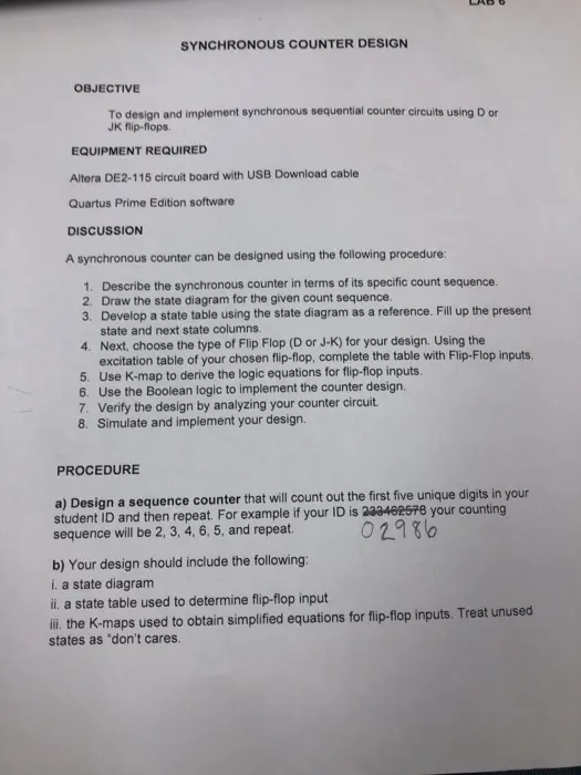
Transcribed Image Text:
SYNCHRONOUS COUNTER DESIGN
OBJECTIVE
To design and implement synchronous sequential counter circuits using D or
JK flip-flops.
EQUIPMENT REQUIRED
Altera DE2-115 circuit board with USB Download cable
Quartus Prime Edition software
DISCUSSION
A synchronous counter can be designed using the following procedure:
1. Describe the synchronous counter in terms of its specific count sequence.
2. Draw the state diagram for the given count sequence.
3. Develop a state table using the state diagram as a reference. Fill up the present
state and next state columns.
4. Next, choose the type of Flip Flop (D or J-K) for your design. Using the
excitation table of your chosen flip-flop, complete the table with Flip-Flop inputs..
5. Use K-map to derive the logic equations for flip-flop inputs.
6. Use the Boolean logic to implement the counter design.
7. Verify the design by analyzing your counter circuit.
8. Simulate and implement your design.
PROCEDURE
a) Design a sequence counter that will count out the first five unique digits in your
student ID and then repeat. For example if your ID is 233402578 your counting
sequence will be 2, 3, 4, 6, 5, and repeat.
b) Your design should include the following:
i. a state diagram
ii. a state table used to determine flip-flop input
02986
iii. the K-maps used to obtain simplified equations for flip-flop inputs. Treat unused
states as "don't cares.
c) Use Altera LPM Counter Megafunction to design a clock source with a frequency
of about 1.5 Hz (see Figure 6-1).
From the symbol libraries choose:
1. Mega Functions > Arithmetic > Ipm_counter
2. Right click on symbol and choose properties.
3. Click on port tab and change the status to unused for all Names except (6) clock
and (10) q.
4. Click on parameter tab and select (5) LPM WIDTH value of 25 and type unsigned
integer. Click OK.
5. Generate pins for ports.
6. Change the output q0 bus width to q [24..0) as shown in Figure 6-1.
LPM COUNTER
Figure 6-1 Altera LPM Counter Megafunction
d) A basic block diagram for the circuit to be built and tested is shown in Figure 6-2.
The clock input to your sequence counter will be 50 MHz/ 225. In Quartus Prime,
connect a wire to clock input of sequence counter, select the wire and right click. Go to
properties and type q24 in the name field.
m) Connect the output of the sequence counter to the 7-segment display and
demonstrate operation of the circuit to your instructor. Use the 50 MHz internal clock
(pin Y2) as the clock source.
purted
7447 and 7-segme
40
LP
Sequence
Counter
display circuit board
1 Hz Clock
Pin 12
cled
Figure 6-2 Sequence Counter Block Diagram
R DESIG
ntial cour
able
followi
of its
seque
am as
K) for
mplet
or flip
unte
er cir
but
ID
LAD
iii K-Map
Q.Q
Q3 Q2
Q302
Q3 Q
Q3 Q2
x
x
Equation Q
QQQQ
Q.Q.
QQ. Q.Q
0
2
x
x
x
w
X
0
12
X
13
14
15
x
x
Y
10
0
0
x
x
Do
Q. Do
Q3Q2
X
X
Q3Qz
X
X
5
7
Q. Qo
о
3
X
0
Q3 Q2
13
15
X
ル
X
$
Q3 Q2
о
1
71
10
X
X
D
Equation: Q+a+ Q
QQ
QR
QQ
Q3 Q2
b
о
X
X
3
0
2
Q3 Q2
X
7
x
12
X
X
19
15
3
X
Χ
Q3 Q2
D₂ Equation: 03.00
QQo
Oz X
о
Go L
QQ Q.Q
QQ
0
4
X
Q3
.
Q3 Q2
2
X
X
5
X
о
QeQz
Q3 Q2
12
"
X
X
*
X
O'
9
1
X
Pz
Equation: QQ
check_circle الجواب — حل مفصل خطوة بخطوة
hourglass_top
🔒
الحل الكامل متاح للمشتركين
اشترك في أرشيف الأسئلة لعرض هذا الحل وآلاف الحلول المفصلة خطوة بخطوة من معلمين معتمدين.