تم الحل ✓
categoryهندسة حاسوب وشبكات
schoolبكالوريوس
event_available2026-07-13
السؤال
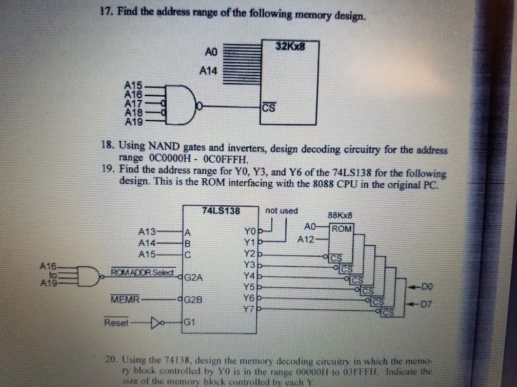
Transcribed Image Text:
17. Find the address range of the following memory design.
AO
A14
32Kx8
A15.
A16
A17
D
A18
A19
CS
18. Using NAND gates and inverters, design decoding circuitry for the address
range 0C0000H-OCOFFFH.
19. Find the address range for Y0, Y3, and Y6 of the 74LS138 for the following
design. This is the ROM interfacing with the 8088 CPU in the original PC.
74LS138
not used
88Kx8
A0- ROM
A13
A
YO
A12
A14-
B
Y1
A15-
C
Y2b
CS
A16-
to
Y3b
ROM ADDR Select
G2A
Y4
A19-
Y5
MEMR
G2B
Y6b-
Y7
Reset
Do
G1
-DO
D7
20. Using the 74138, design the memory decoding circuitry in which the memo-
ry block controlled by YO is in the range 00000H to 03FFFH. Indicate the
size of the memory block controlled by each Y
check_circle الجواب — حل مفصل خطوة بخطوة
hourglass_top
🔒
الحل الكامل متاح للمشتركين
اشترك في أرشيف الأسئلة لعرض هذا الحل وآلاف الحلول المفصلة خطوة بخطوة من معلمين معتمدين.