تم الحل ✓
categoryهندسة حاسوب وشبكات
schoolبكالوريوس
event_available2026-07-13
السؤال
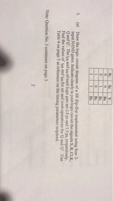
Transcribed Image Text:
S₁
So
Y
0
0
De
0
1
Di
1
0
D₂
1
1
Dj
3. (a) Draw the logic circuit diagram of a SR flip-flop implemented using four 2-
input NAND gates. Indicate clearly in your logic circuit the signals S, R, CLK,
Q and Q'. The tpth and tph of each logic gate are 2.8 ps and 3.5 ps, respectively.
Find the values of tpth and tphl for set and reset operations for Q and Q'. Use
Table 4 on page 3 as reference on the timing parameters required.
Note: Question No. 3 continues on page 3.
2
ATTENTION: The Singapore Copyright Act applies to the use of this document. Nanyang Technological University Library
EE2004/IM1004
Table 4
10
Output (operation)
Q (set)
tpth(ps)
Iphi(ps)
5.6ps
이
Q(reset)
17.52
ΟΙ
10
Q' (set)
Q'(reset)
7
14
(12 Marks)
(b) Referring to the memory chip shown in Figure 1, answer the following
questions.
(i)
Specify if the memory chip shown is a DRAM or SRAM. Indicate the
size of the memory chip.
check_circle الجواب — حل مفصل خطوة بخطوة
hourglass_top
🔒
الحل الكامل متاح للمشتركين
اشترك في أرشيف الأسئلة لعرض هذا الحل وآلاف الحلول المفصلة خطوة بخطوة من معلمين معتمدين.