تم الحل ✓
categoryالهندسة الكهربائية
schoolبكالوريوس
event_available2026-07-15
السؤال
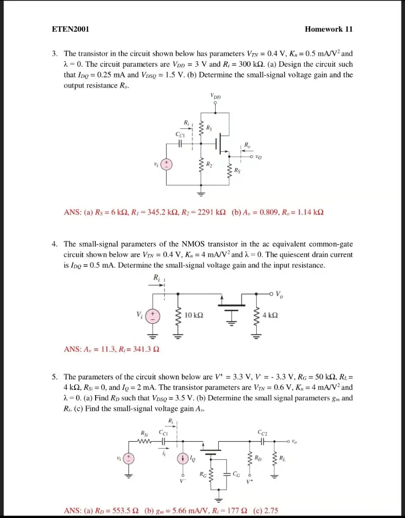
Transcribed Image Text:
ETEN2001
Homework 11
3. The transistor in the circuit shown below has parameters Vry = 0.4 V, KI = 0.5 mA/V² and
λ= 0. The circuit parameters are VDD = 3 V and R₁ = 300 k2. (a) Design the circuit such
that Ipo = 0.25 mA and Vosg = 1.5 V. (b) Determine the small-signal voltage gain and the
output resistance Ro.
VDD
ANS: (a) Rs = 6 k2, R = 345.2 k2, R2=2291 k2 (b) A. = 0.809, Ro= 1.14 ks2
4. The small-signal parameters of the NMOS transistor in the ac equivalent common-gate
circuit shown below are VTN = 0.4 V, K = 4 mA/V2 and 2 = 0. The quiescent drain current
is IDQ = 0.5 mA. Determine the small-signal voltage gain and the input resistance.
R₁
ANS: A,, = 11.3, R;= 341.3 2
10 ΚΩ
ww
4 ΚΩ
5. The parameters of the circuit shown below are V+ = 3.3 V, V = -3.3 V, RG = 50 kQ, RL =
4 k2, Rs; = 0, and Io = 2 mA. The transistor parameters are Vrv = 0.6 V, K = 4 mA/V² and
λ= 0. (a) Find RD such that Vpsg = 3.5 V. (b) Determine the small signal parameters g and
Ri. (c) Find the small-signal voltage gain Av.
Rsi
CCI
RG
CC2
Ve
RL
ANS: (a) Rp 553.5 2 (b) gm = 5.66 mA/V, R = 177 2 (c) 2.75
check_circle الجواب — حل مفصل خطوة بخطوة
hourglass_top
🔒
الحل الكامل متاح للمشتركين
اشترك في أرشيف الأسئلة لعرض هذا الحل وآلاف الحلول المفصلة خطوة بخطوة من معلمين معتمدين.