تم الحل ✓
categoryهندسة كهربائية
schoolبكالوريوس
event_available2026-07-15
السؤال
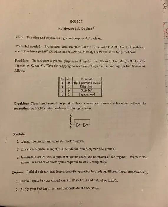
Transcribed Image Text:
ECE 327
Hardware Lab Design 2
Aim: To design and implement a general purpose shift register.
Material needed: Protoboard, logic template, 74175 D-FF's and 74153 MUXes, DIP switches,
a set of resistors (0.25W 1K Ohms and 0.25W 330 Ohms), LED's and wires for protoboard.
Problem: To construct a general purpose 4-bit register. Let the control inputs (to MUXes) be
denoted by So and S₁. Then the mapping between control input values and register functions is as
follows.
So S1
0
Function
0 Hold previous value
0
1
Shift right
1
0
Shift left
1
1
Parallel load
18
Clocking: Clock input should be provided from a debounced source which can be achieved by
connecting two NAND gates as shown in the figure below.
Prelab:
1. Design the circuit and draw its block diagram.
2. Draw a schematic using chips (include pin numbers, Vcc and ground).
3. Generate a set of test inputs that would check the operation of the register. What is the
minimum number of clock cycles required to test it completely?
Demo: Build the circuit and demonstrate its operation by applying different input combinations.
1. Derive inputs to your circuit using DIP switches and output on LED's.
2. Apply your test input set and demonstrate the operation.
check_circle الجواب — حل مفصل خطوة بخطوة
hourglass_top
🔒
الحل الكامل متاح للمشتركين
اشترك في أرشيف الأسئلة لعرض هذا الحل وآلاف الحلول المفصلة خطوة بخطوة من معلمين معتمدين.